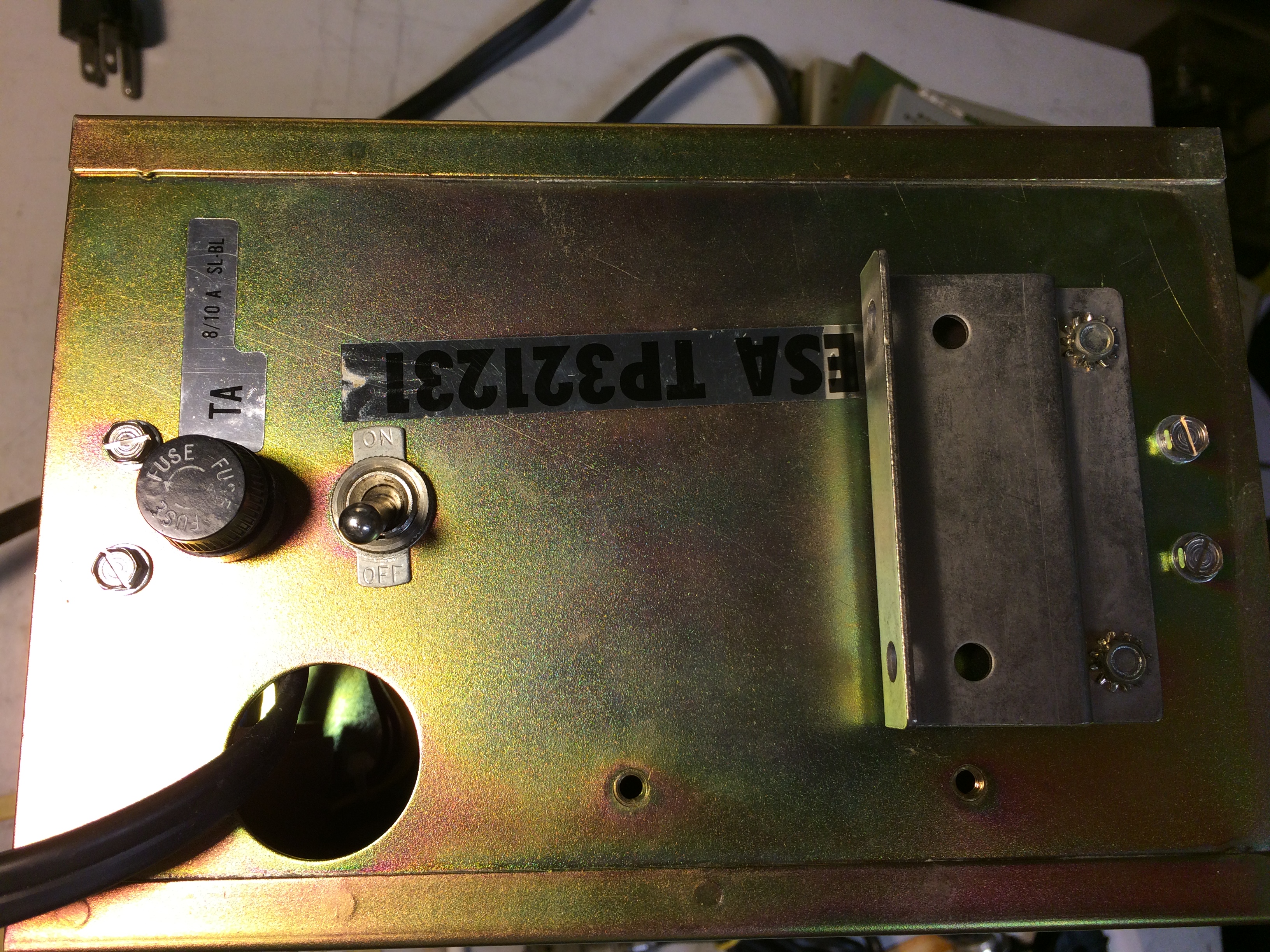
| ESA Electronic Service Assembly (outer shield)  |
ESA Electronic Service Assembly (inner shield) 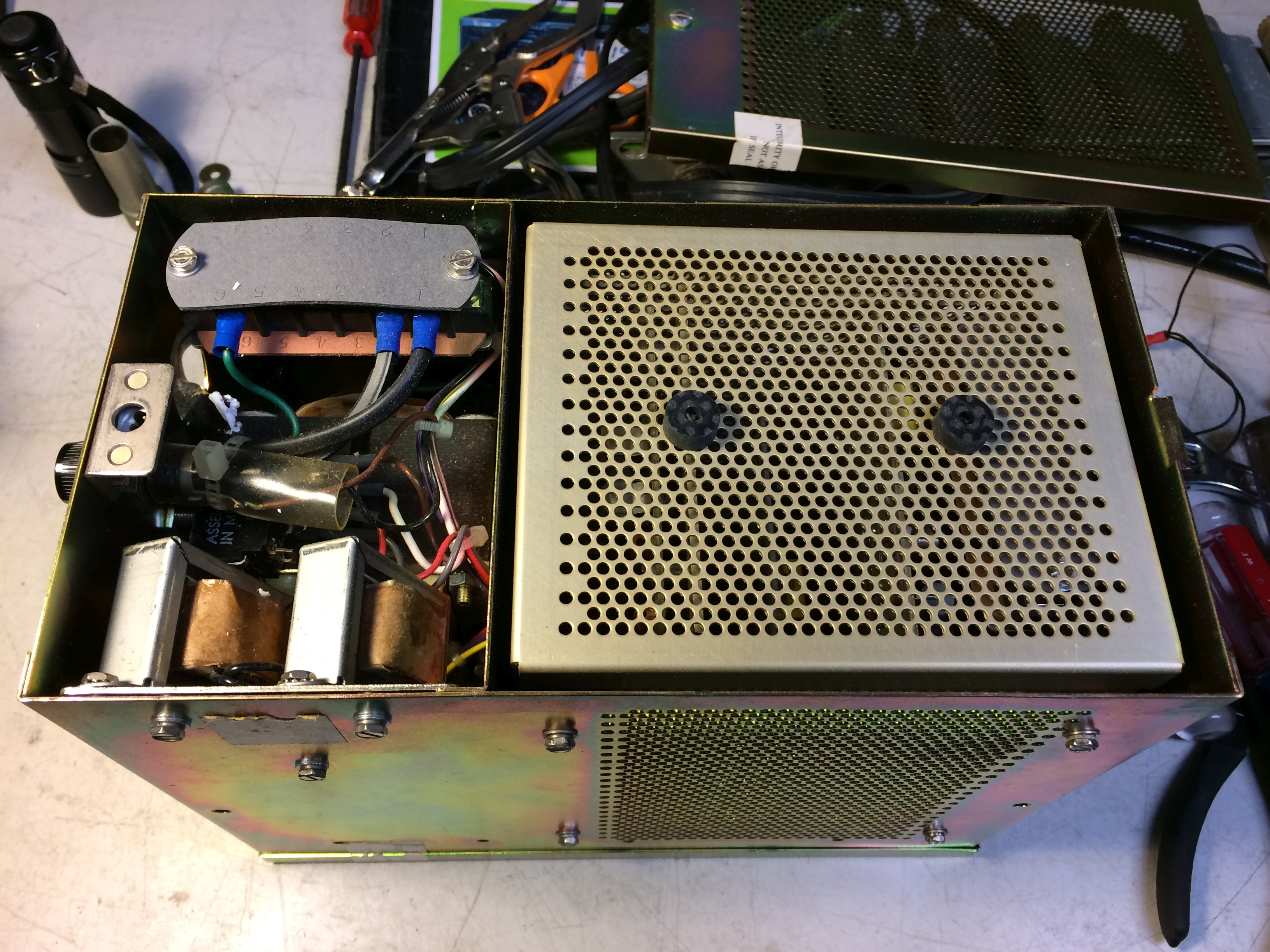 |
ESA Electronic Service Assembly (card slots)  |
ESA Electronic Service Assembly (bottom) 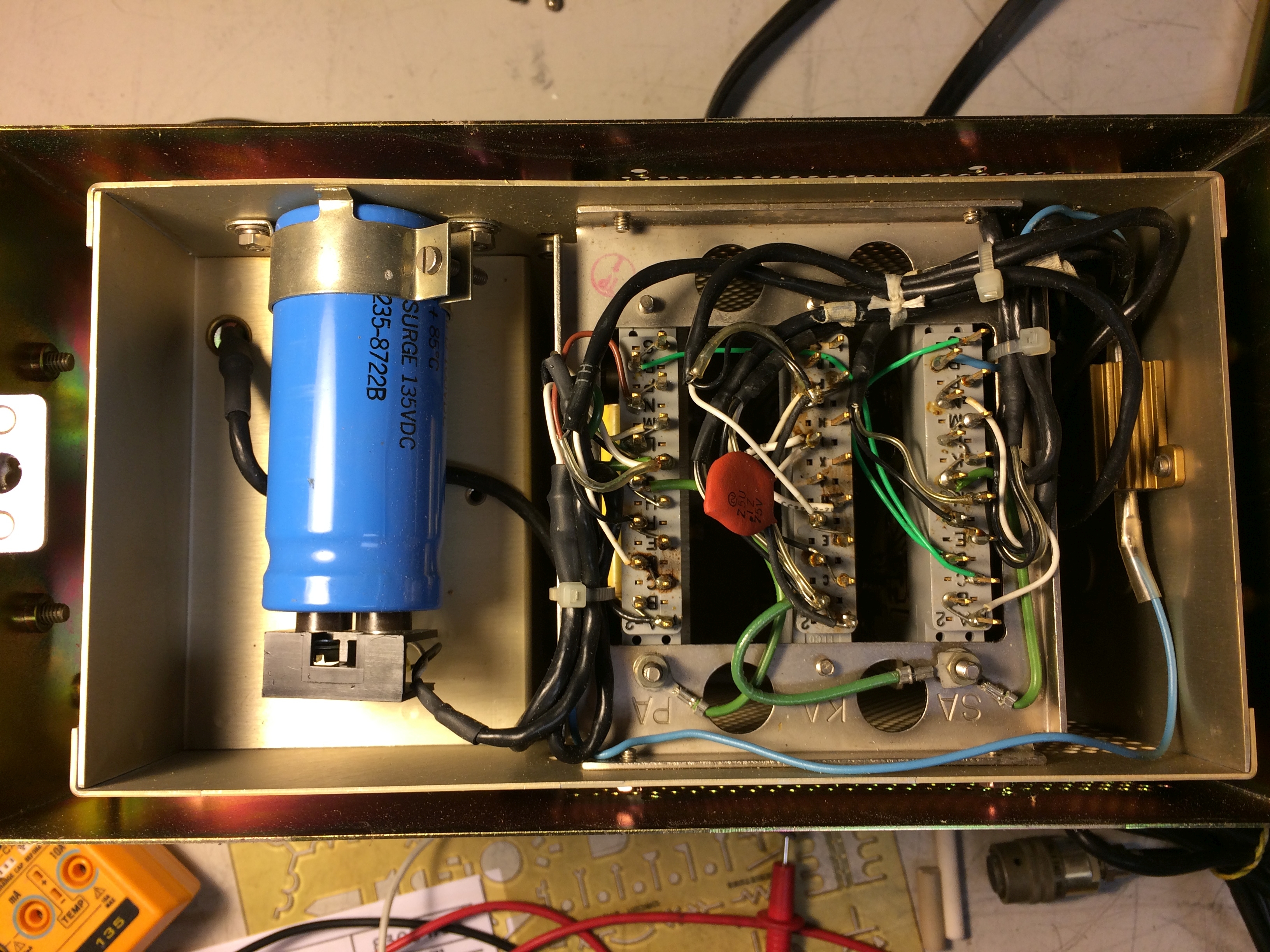 |
 |
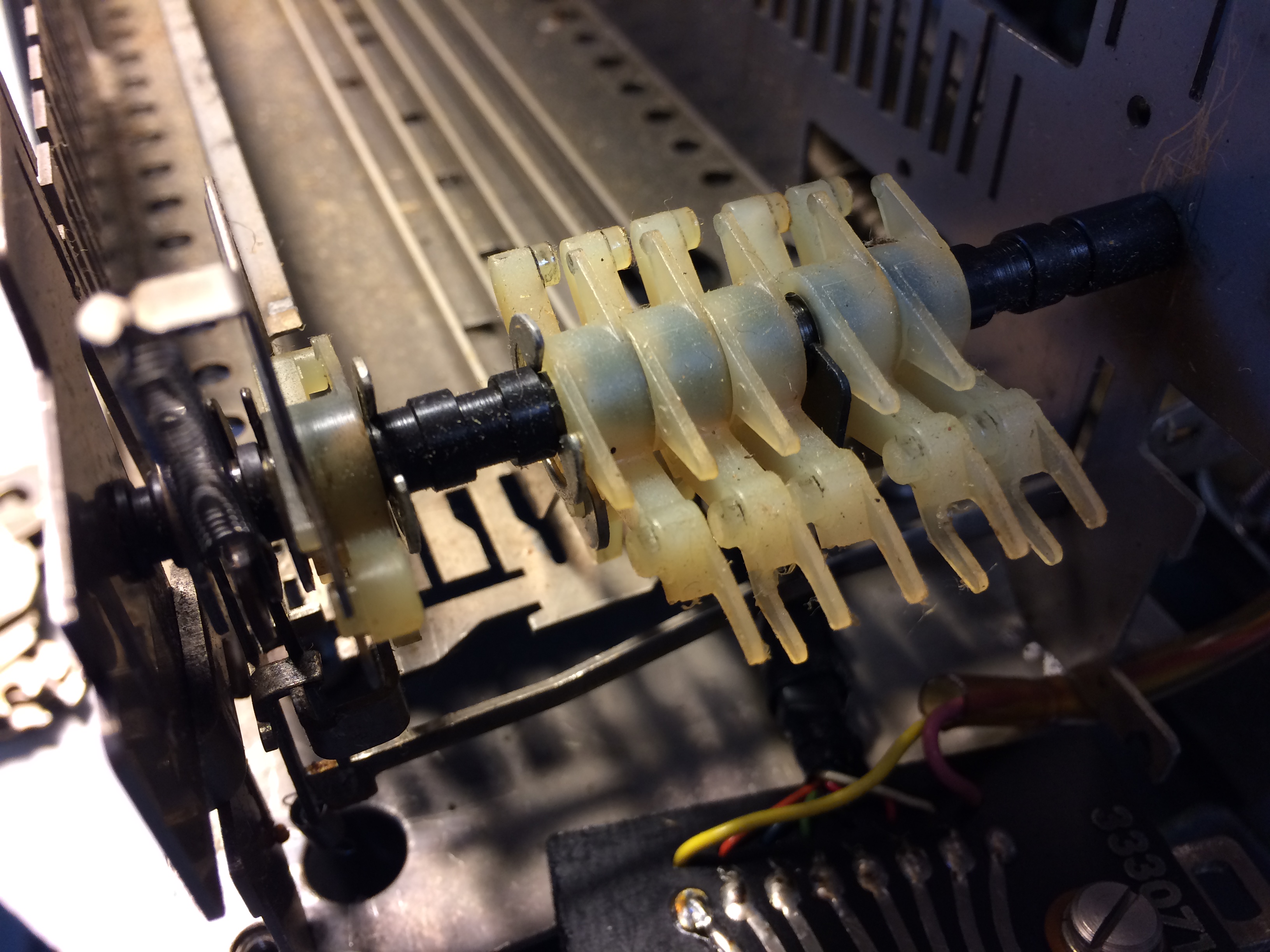
ESA Electronic Service Assembly (Low-Level Signal connections) 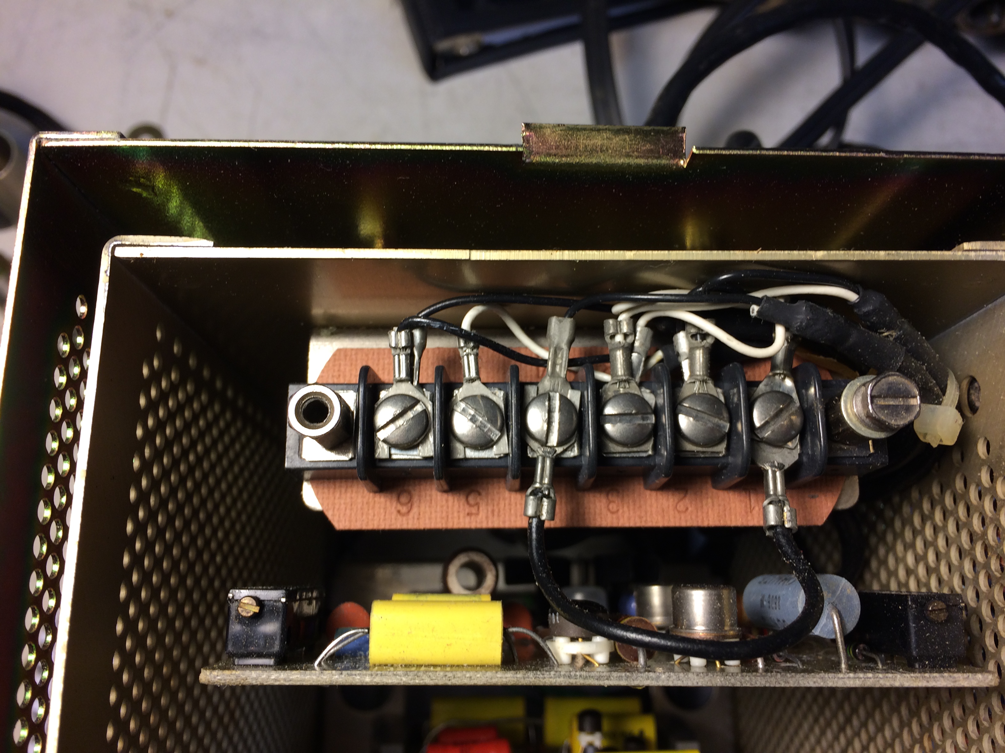 |
323130 Low Level Keyer |
323130 Low Level Keyer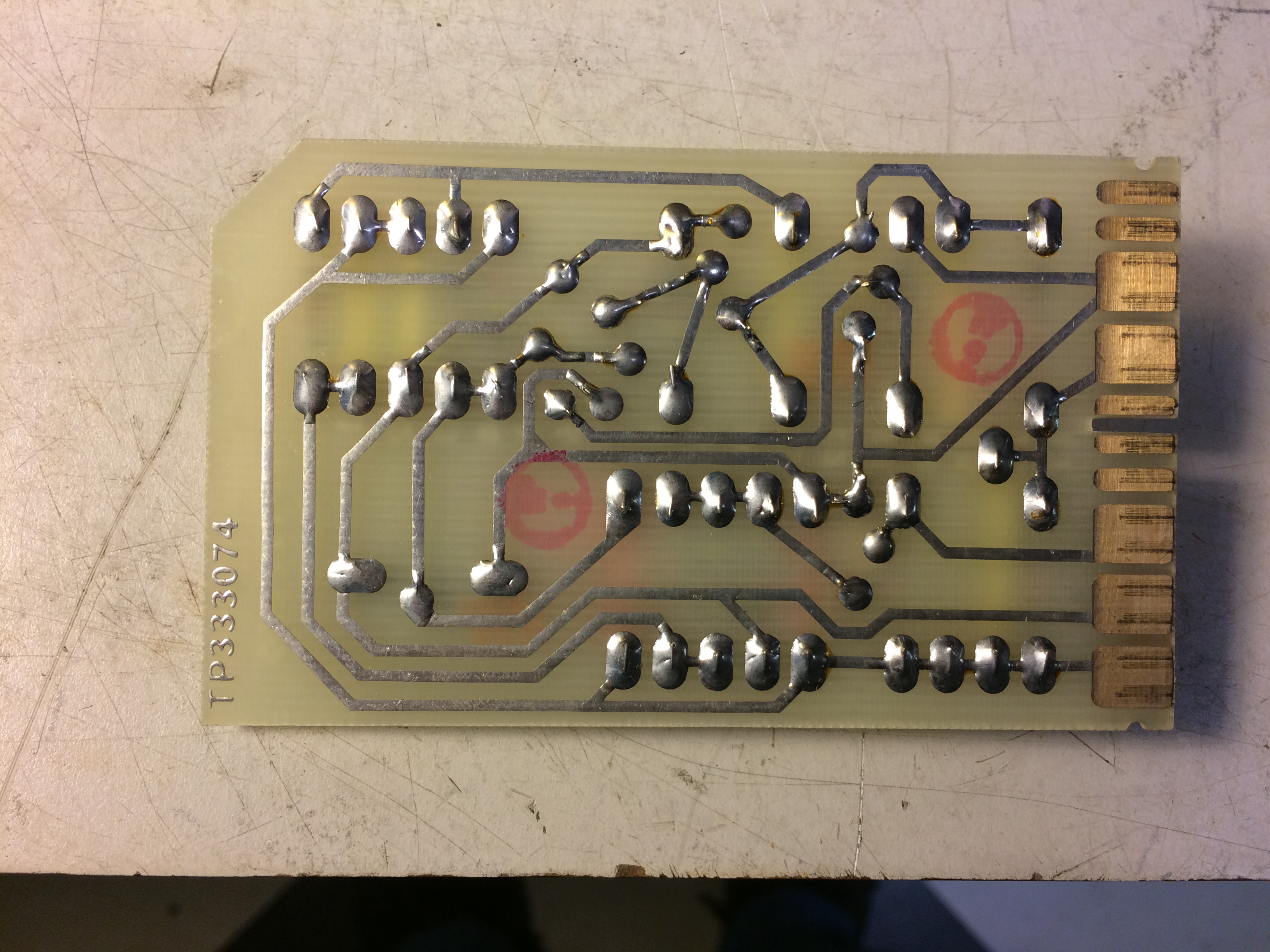 |
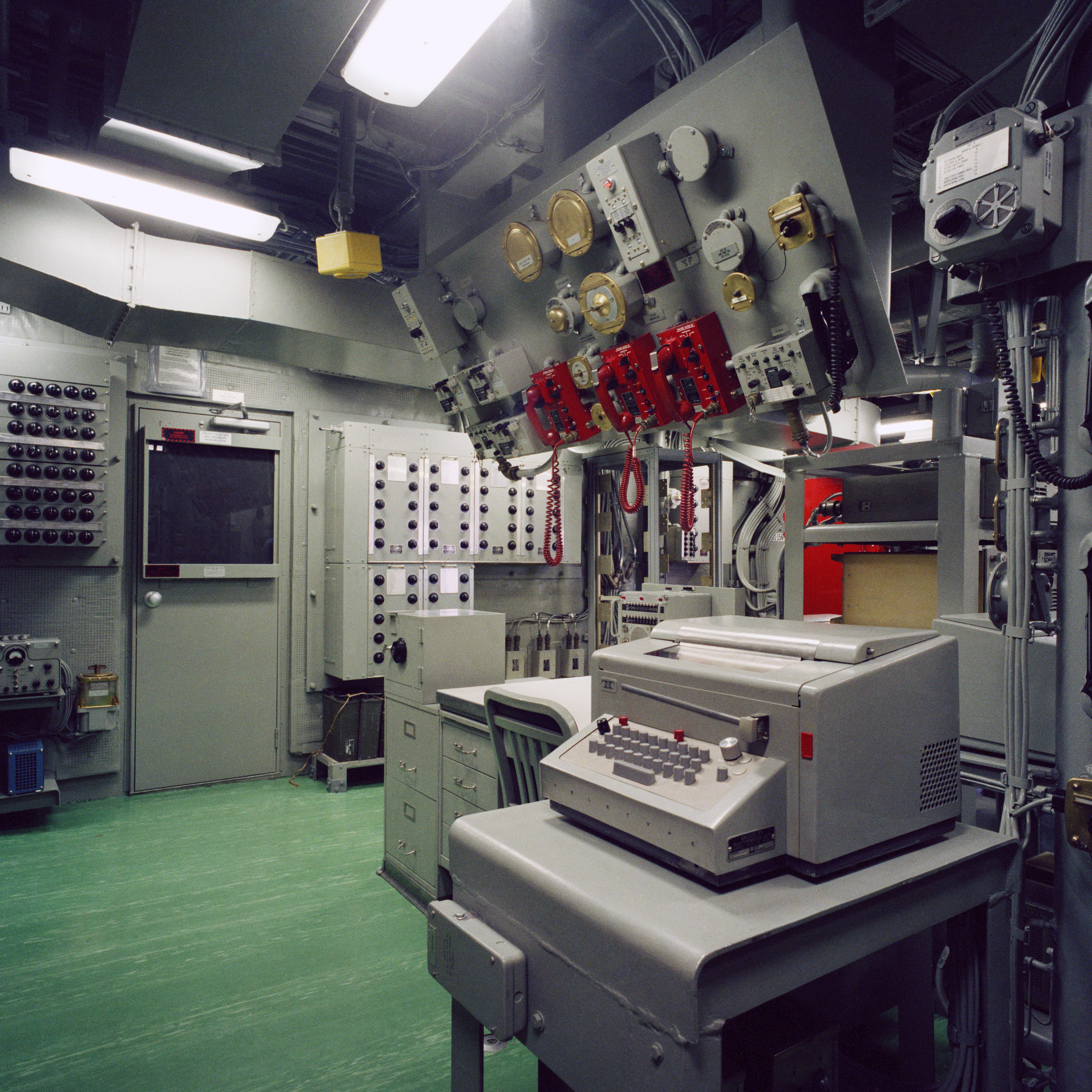
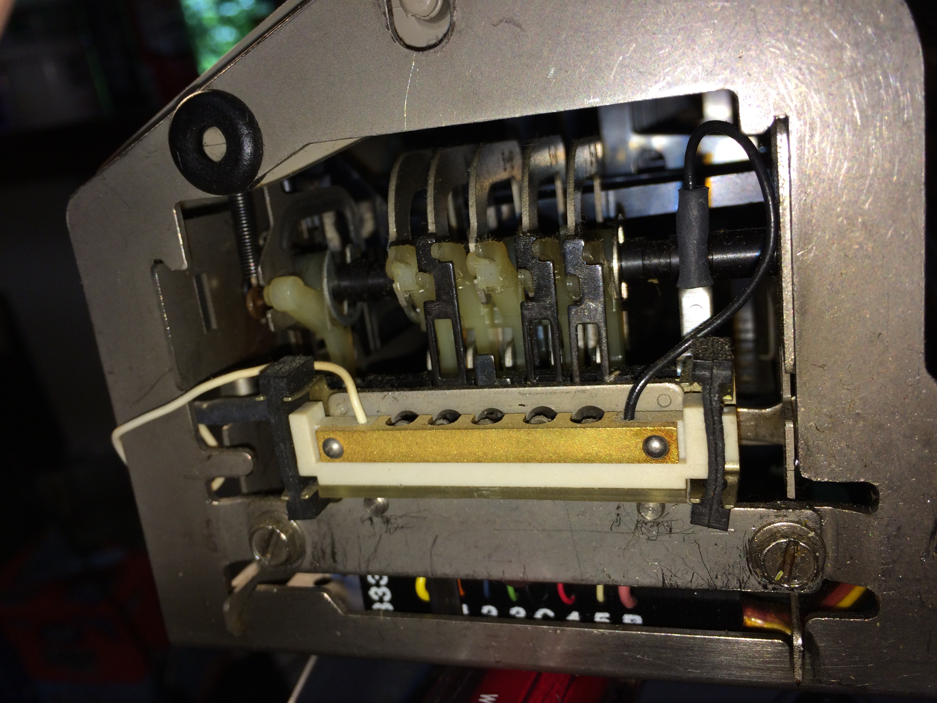
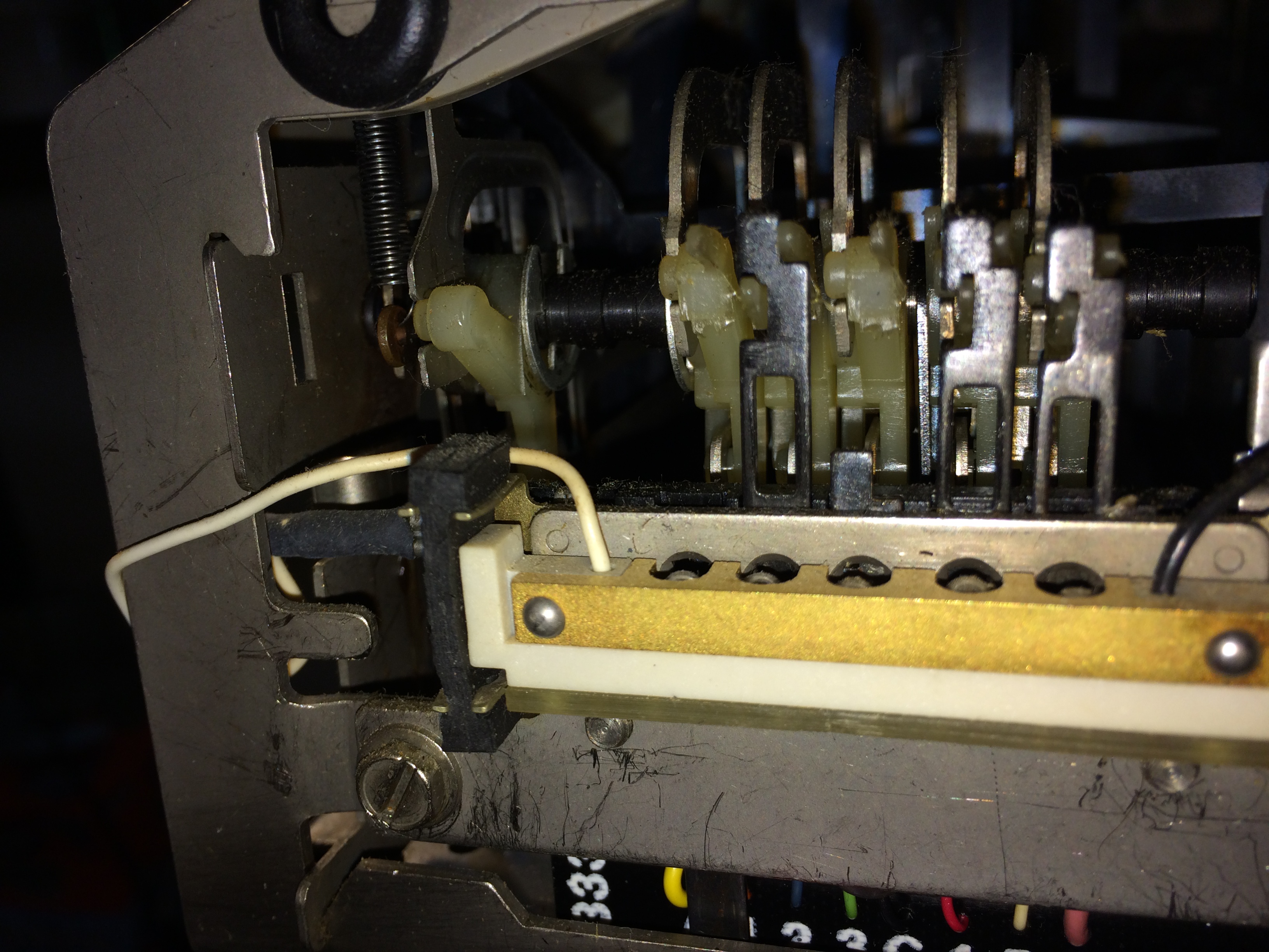
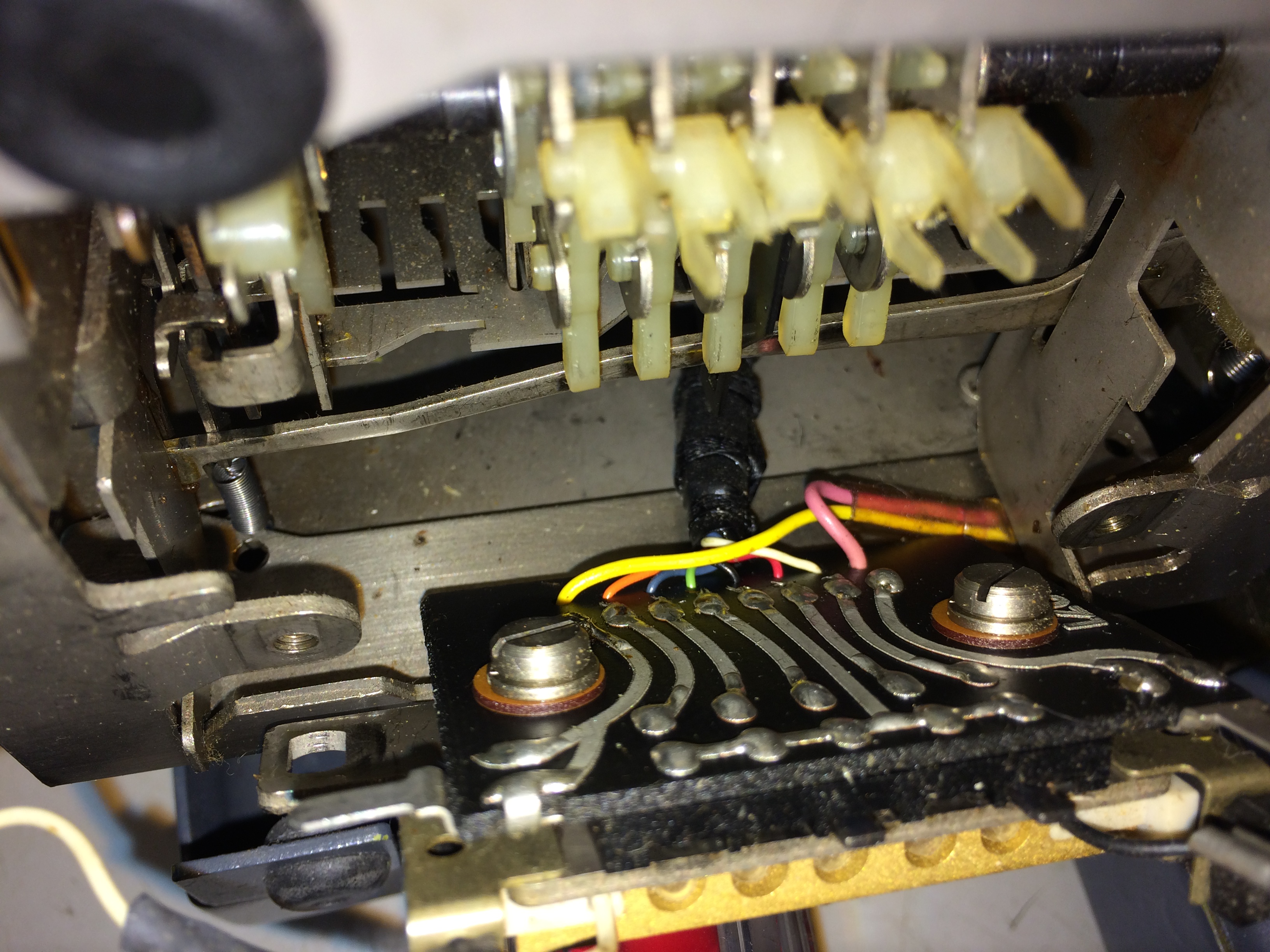
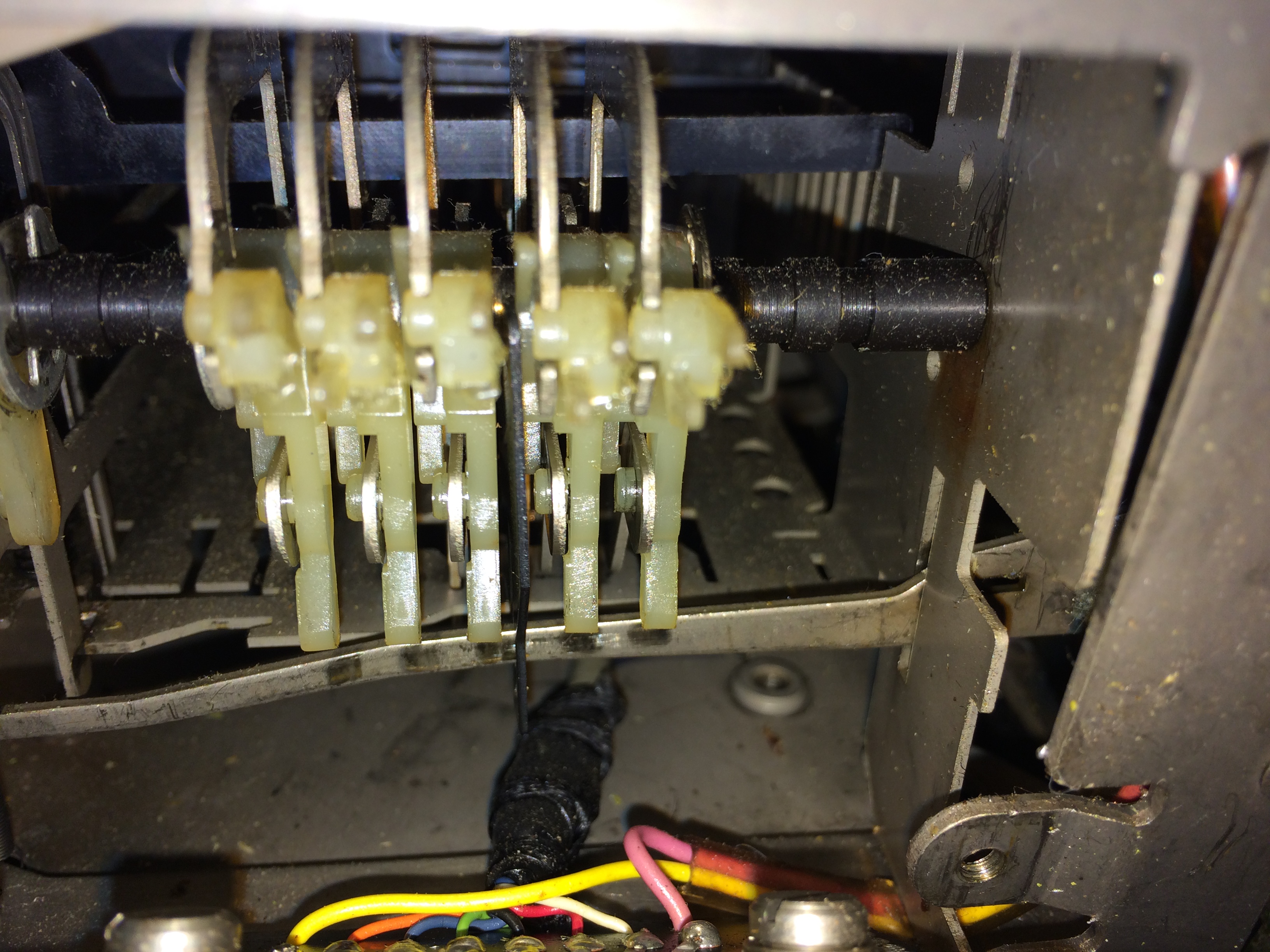
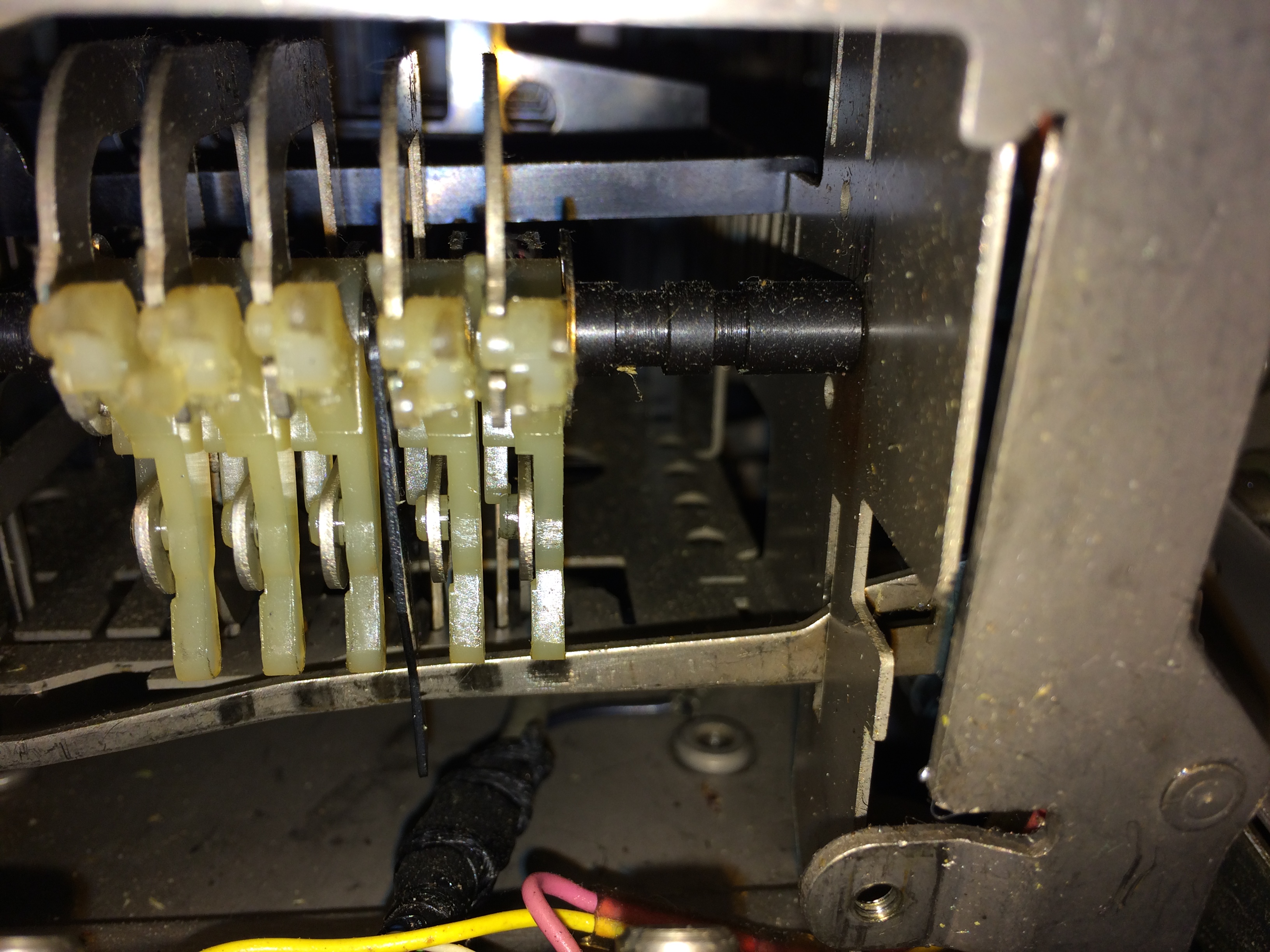
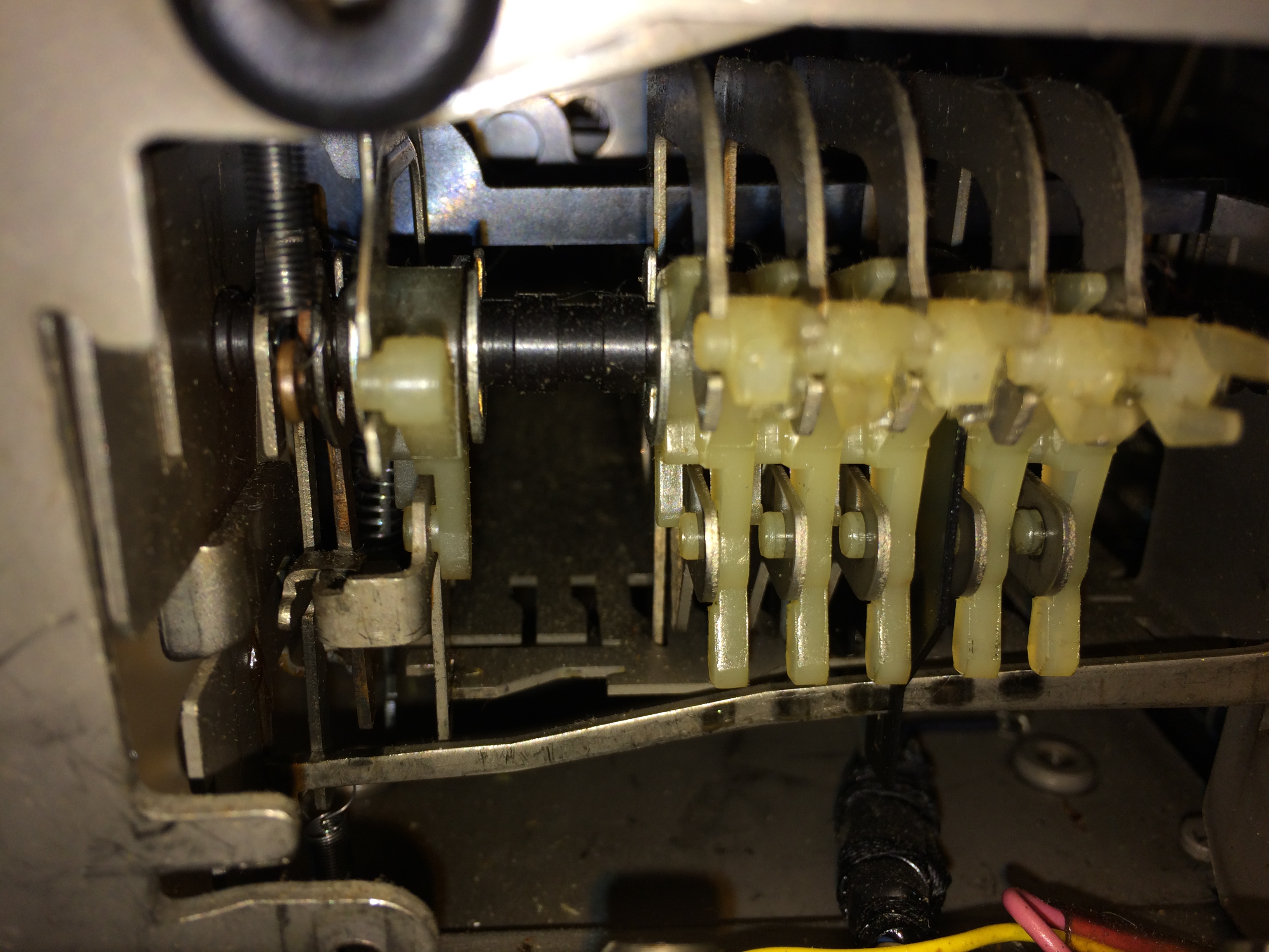
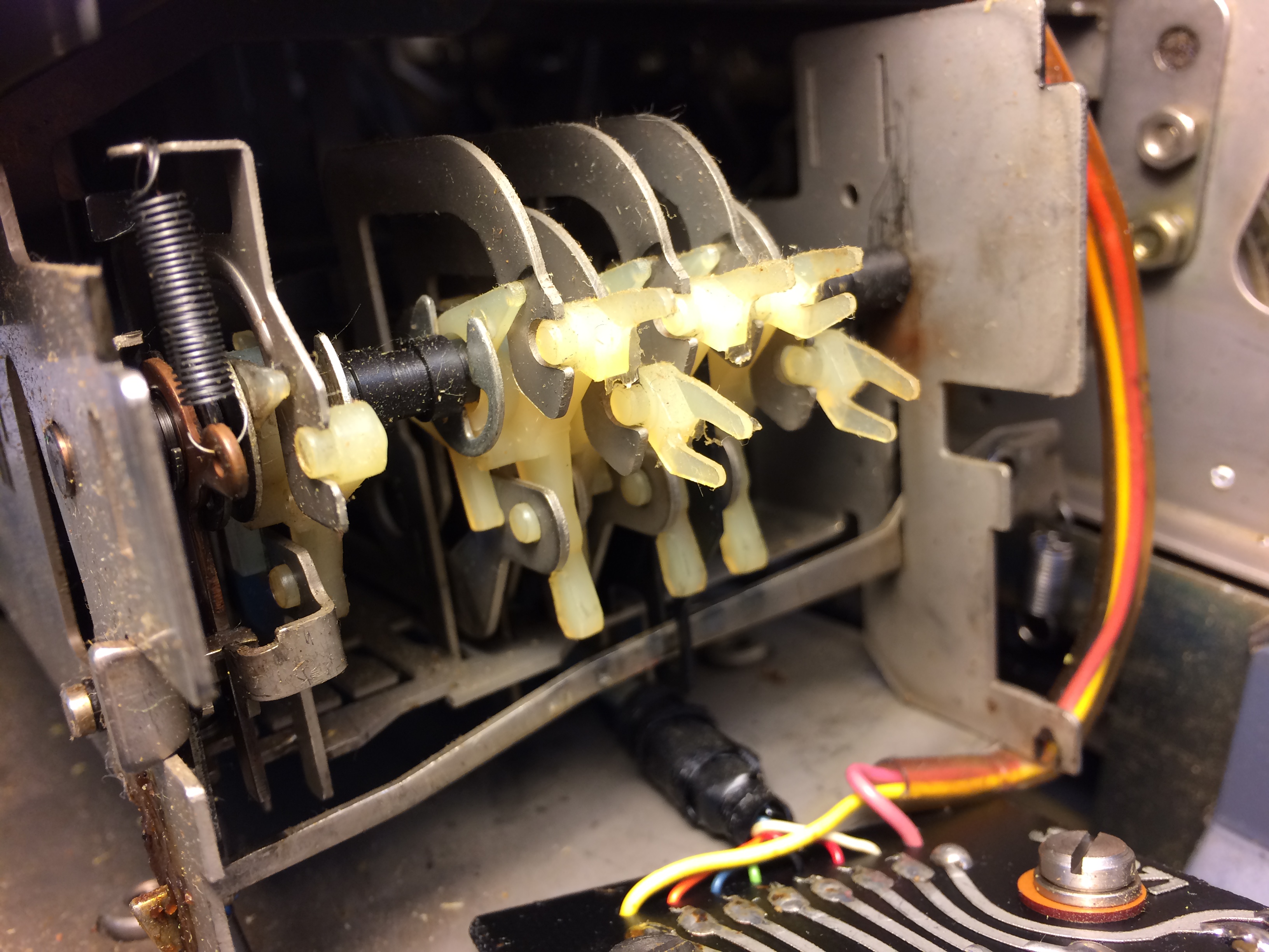
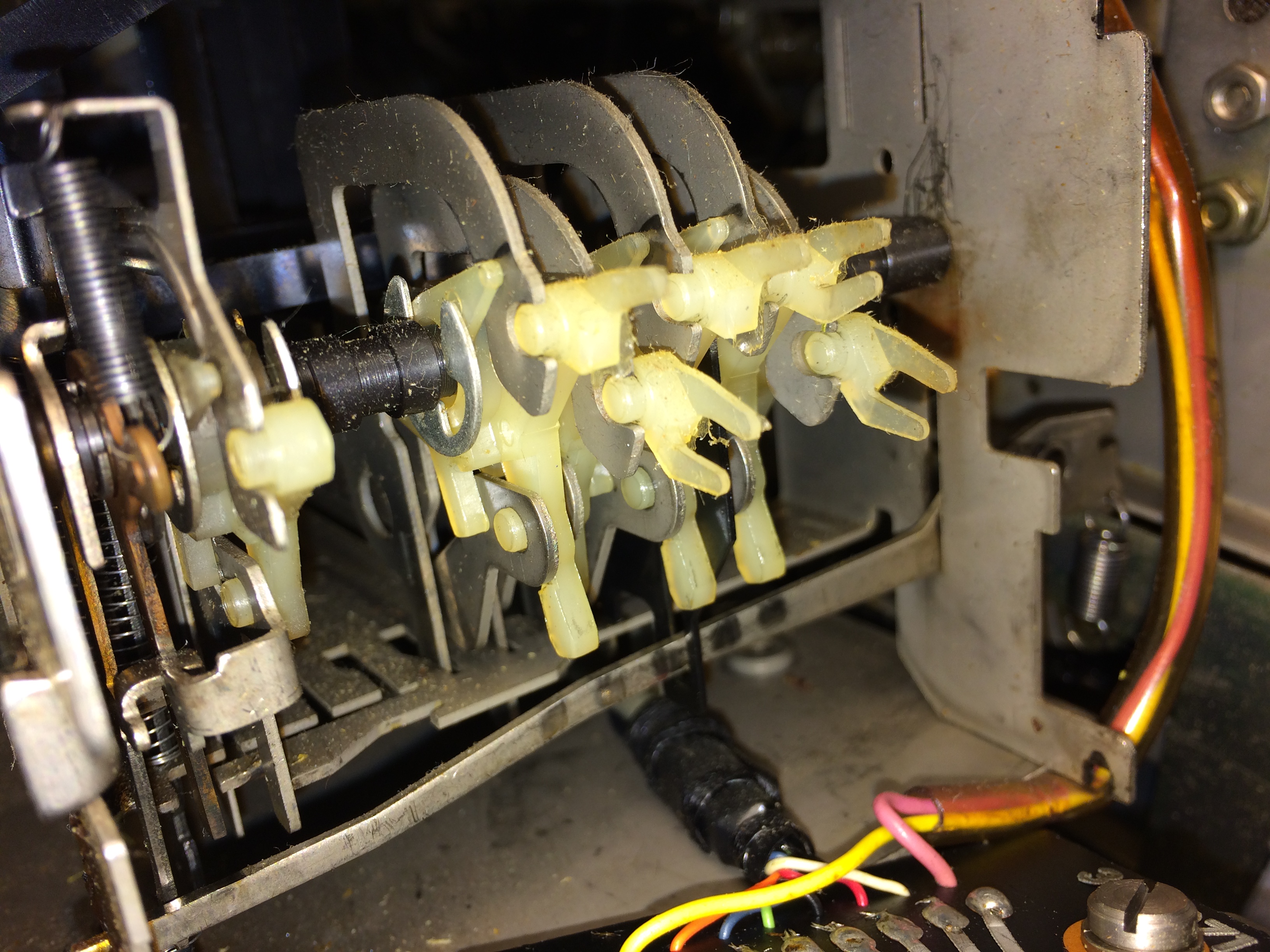
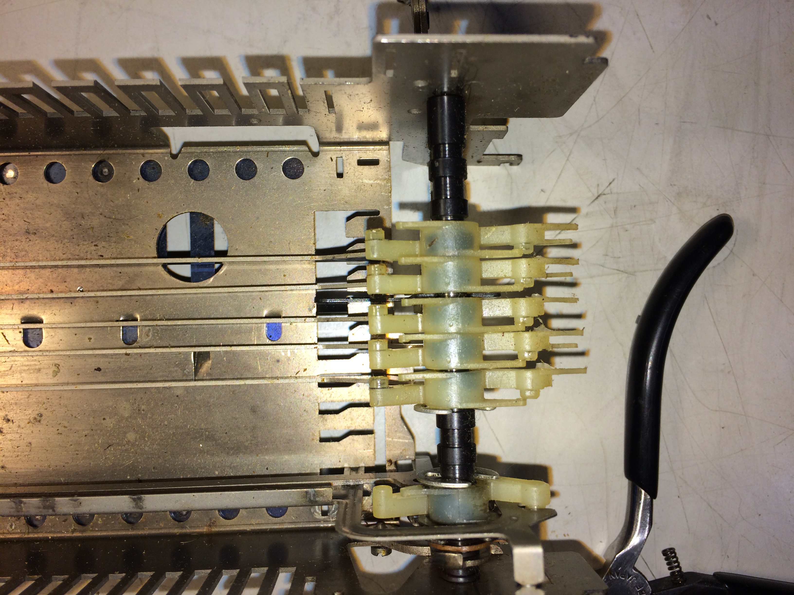
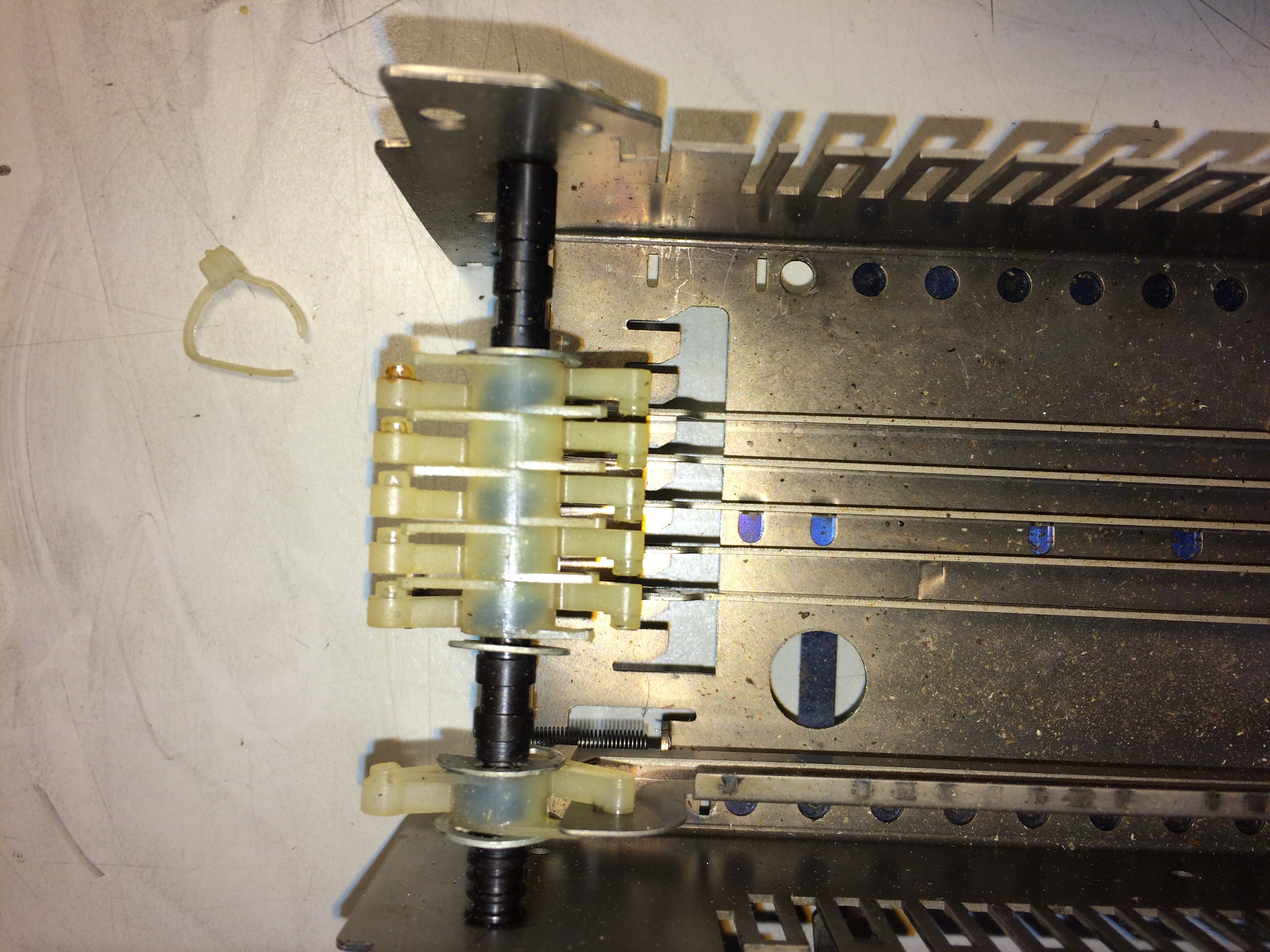
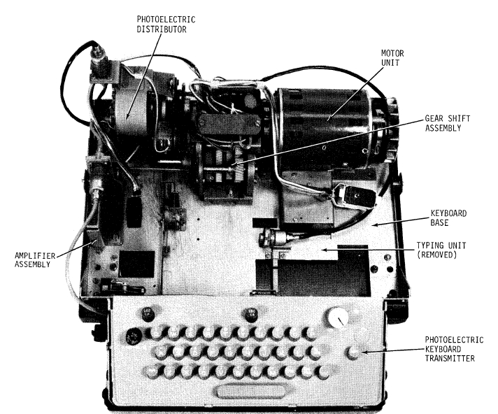
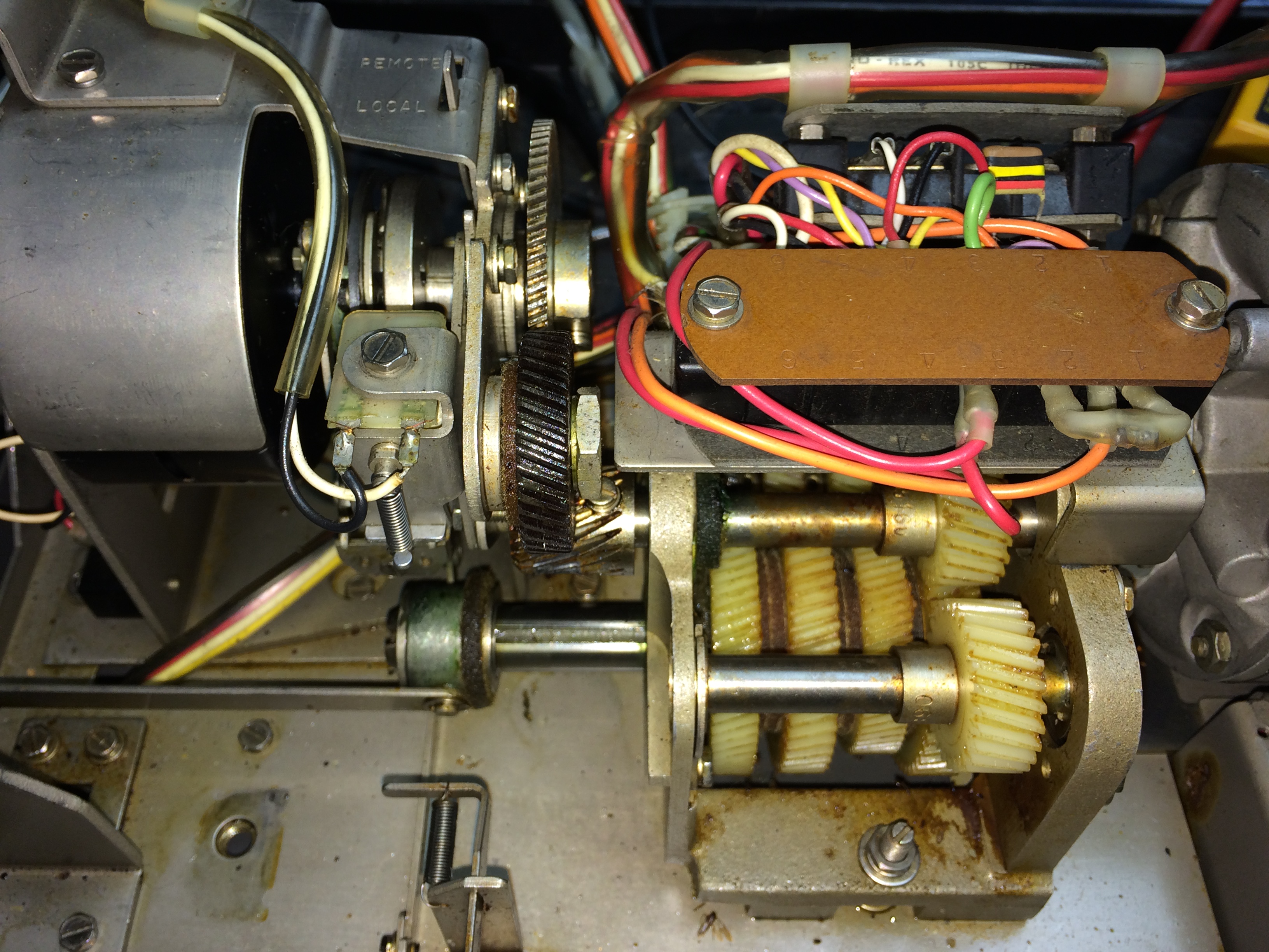
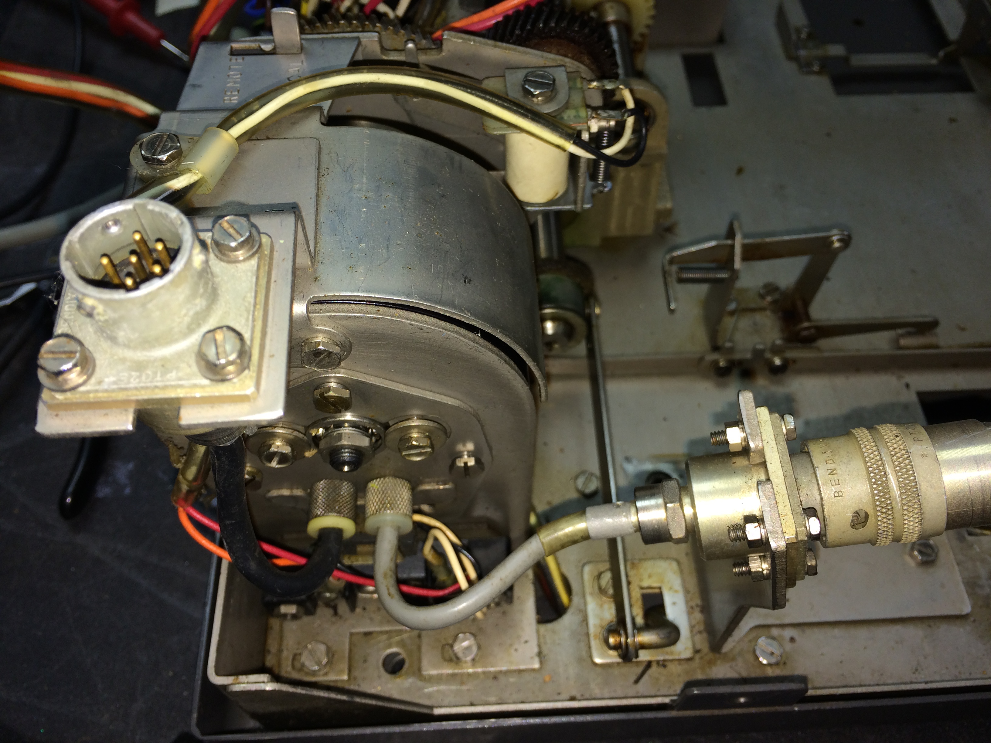
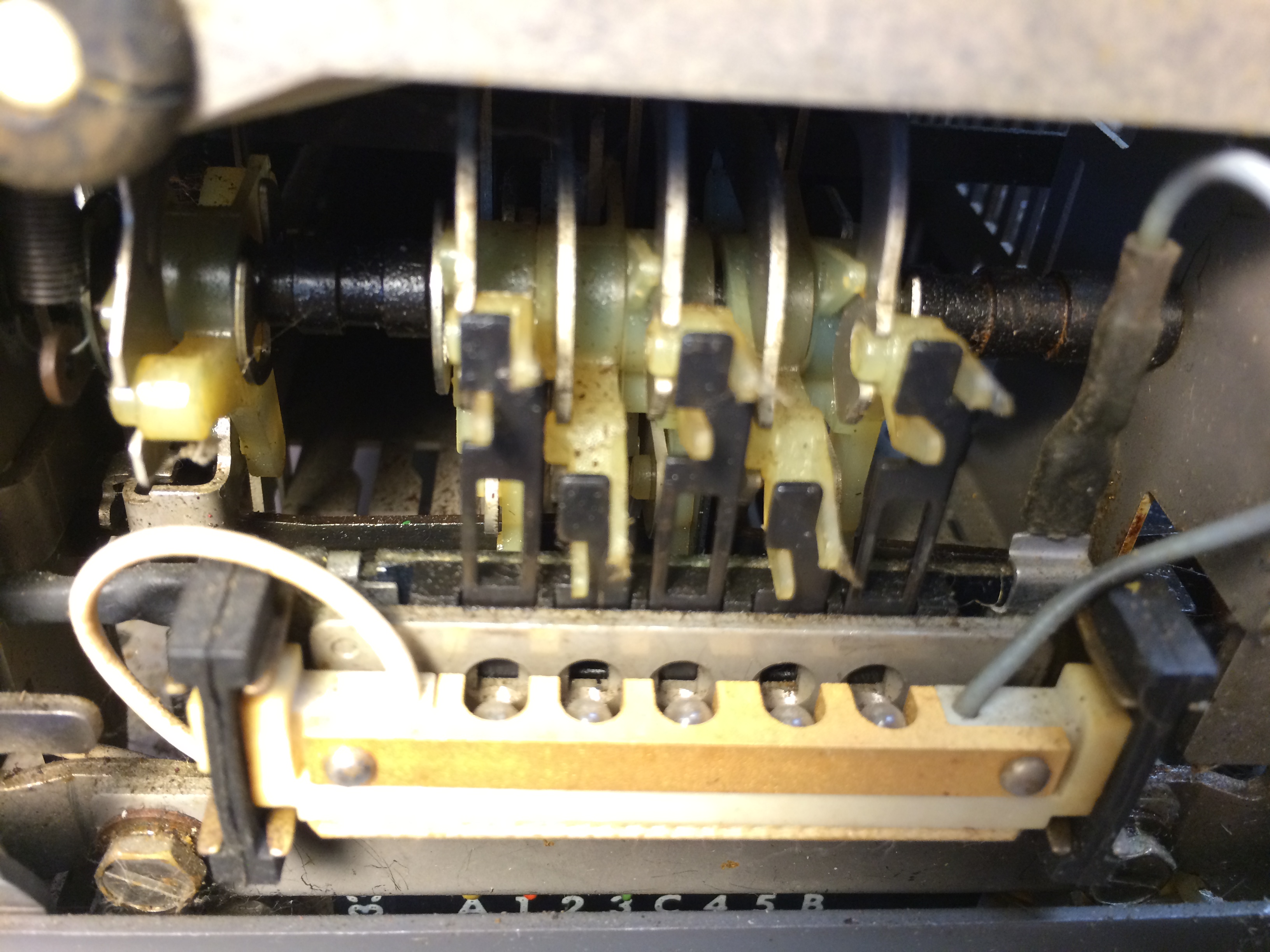
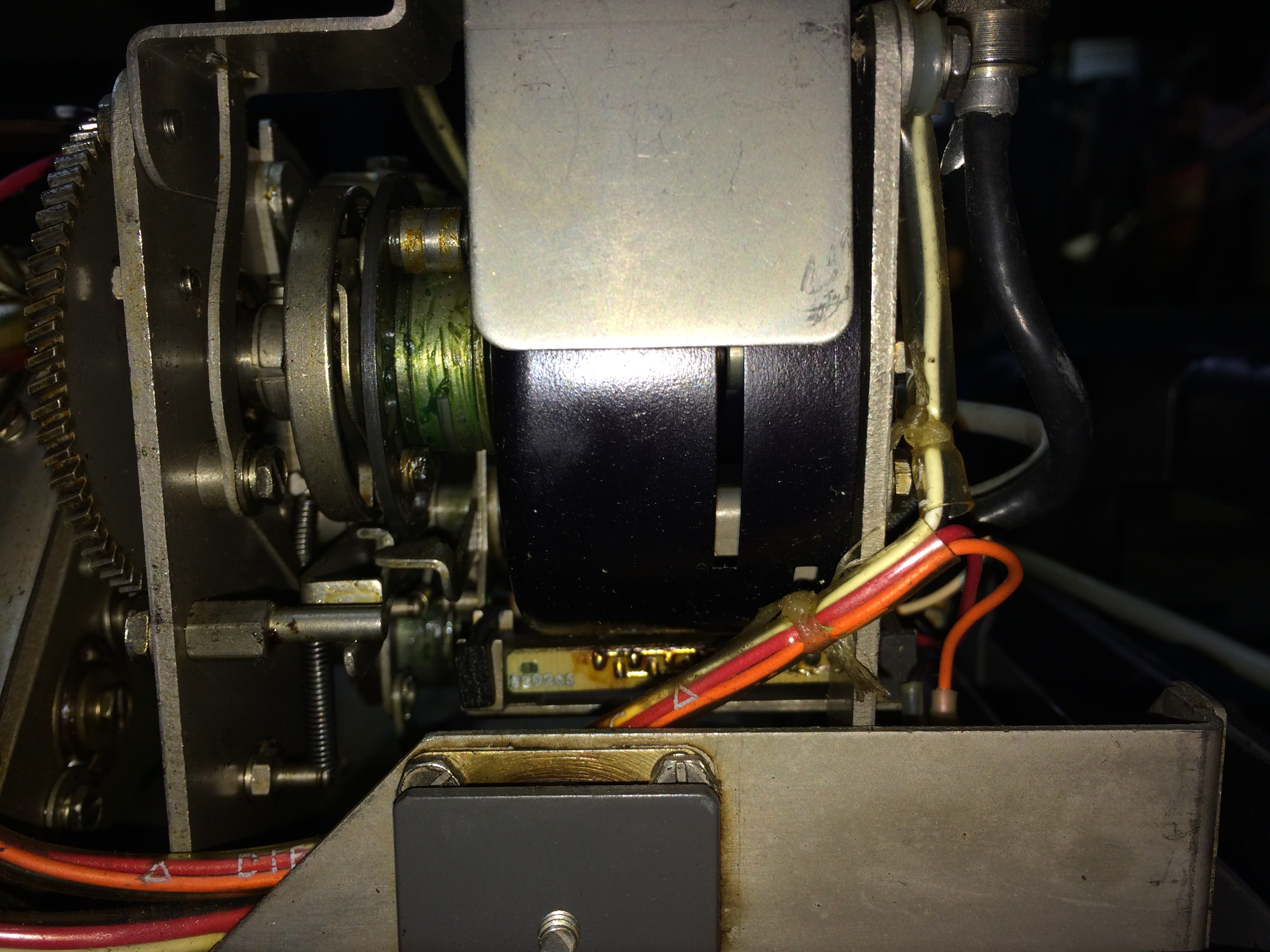
The signal generating mechanism utilizes photoelectric cells instead of a contact mechanism to generate a signal. A lamp assembly provides the necessary light source to electrically activate the cells. A mechanical shutter assembly, linked with the keyboard codebars and located between the photocells and lamp assembly, provides windows to either allow light from the light assembly to pass and activate the cells (mark) or block the light and not activate the cells (space). The photocells will generate a parallel electrical signal of approximately 300 microamperes (ua). The generated signal travels along a shielded cable to a photoelectric distributor. The photoelectric distributor serializes the signal, and by means of shielded cables, routes it to the input of a polar line keyer.
Official Wiring Diagrams - My schematic
The 323130 LLK (Low Level Keyer) is for use in photoelectric systems (such as 28/32 keyboard) requiring a low-level interface and extreme RFI suppression.
The 323130 keyer takes a 250 ua (min) photocell signal from the distributor and by means of passive and active filtering, shapes the output. It is used in conjunction with a 333069 CMD (Clutch Magnet Driver) when the UGC-77 is remotely synchronized.
Circuit Description - In the marking state (photocell illuminated), Q5 is turned off causing the bases of Q1 and Q2 to go positive through the passive shaping network made up of R2, Cl and R4. With the bases of Q1 and Q2 positive, Q1 will turn on turning Q4 off and Q2 will turn off turning Q3 on. Capacitor C2, resistor R6, R9, and capacitor C 3 further shape the wave by providing feedback and phase shift thereby controlling the rate at which the active filter Ql, Q2, Q3, Q4 will switch.
In the spacing state (photocell dark), Q5 is turned on providing a negative signal to the bases of Q1 and Q2. The switching occurs as above except, transistors that are off turn on and those that are on turn off.
During the transition from on to off and off to on, one of the output transistors of the active filter is always conducting. This will provide a smooth transition from plus volts through 0 volts to minus volts and back again. The rate of switching being controlled by the feedback and phase shift of C2, R6 , R9 and C3.
Diode CR1 compensates for the non-symmetry of the first stage. Resistors R10 and R5 and capacitors C6 and C7 provide for the proper output impedance and some additional shaping.


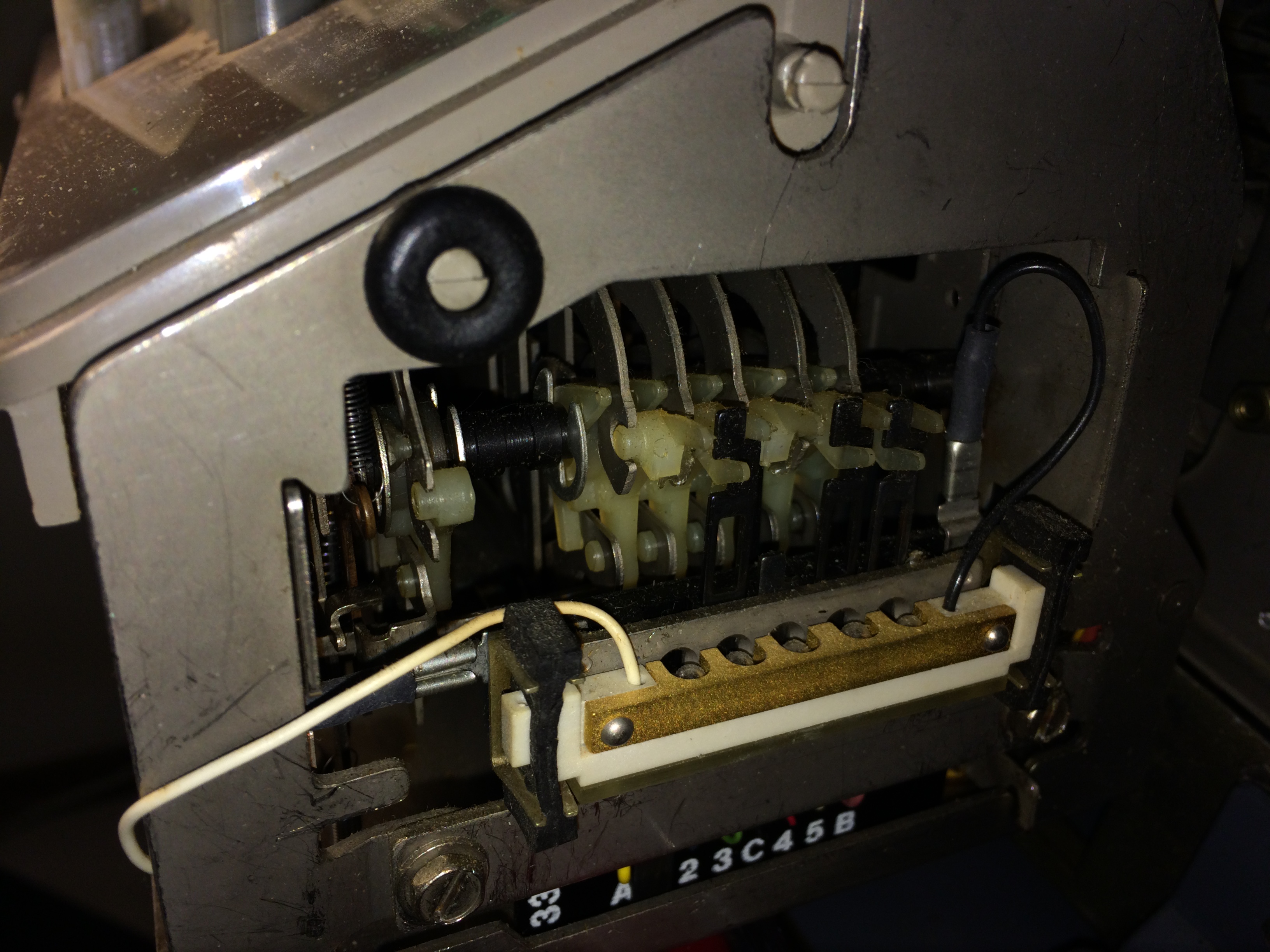
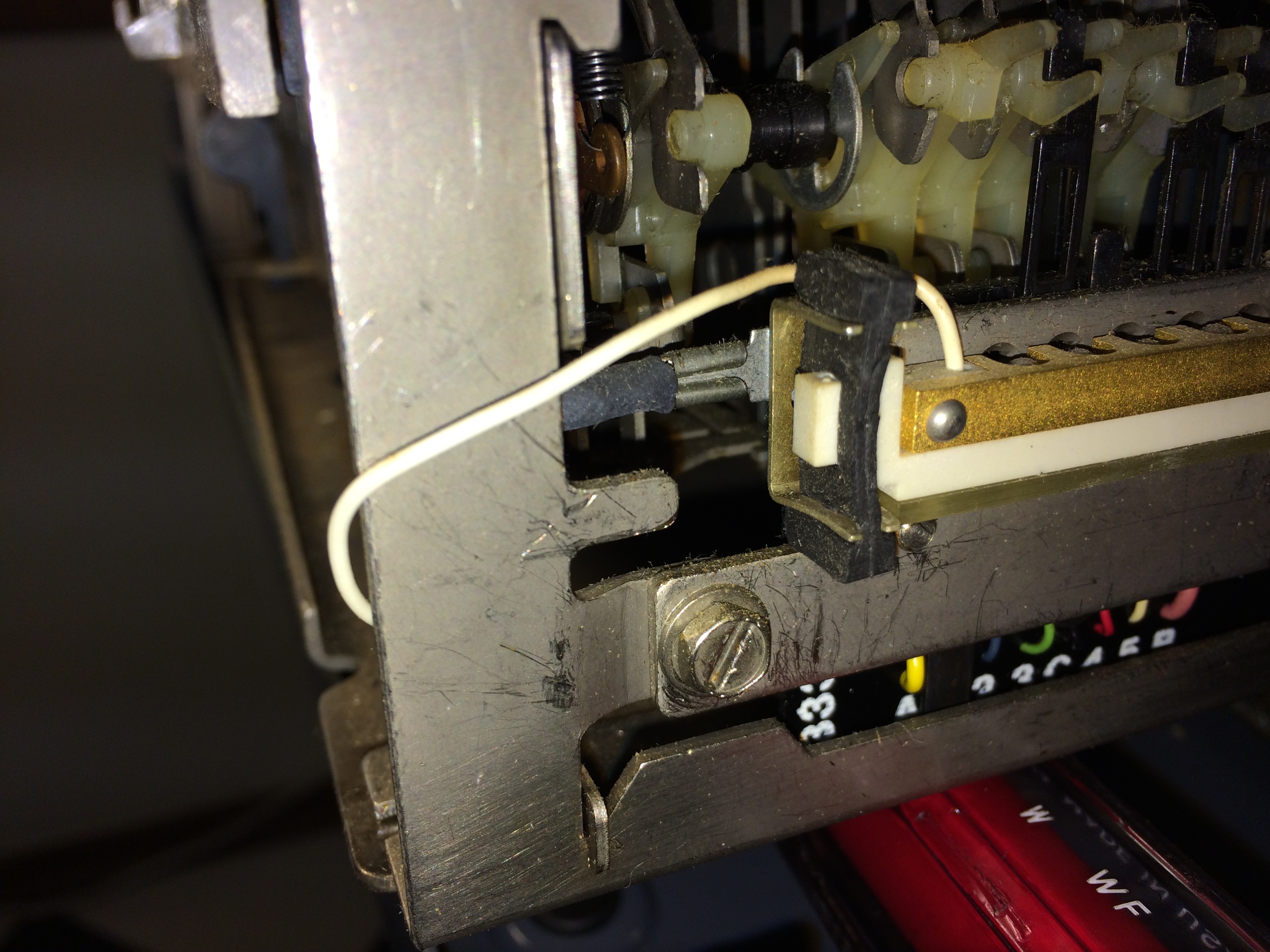
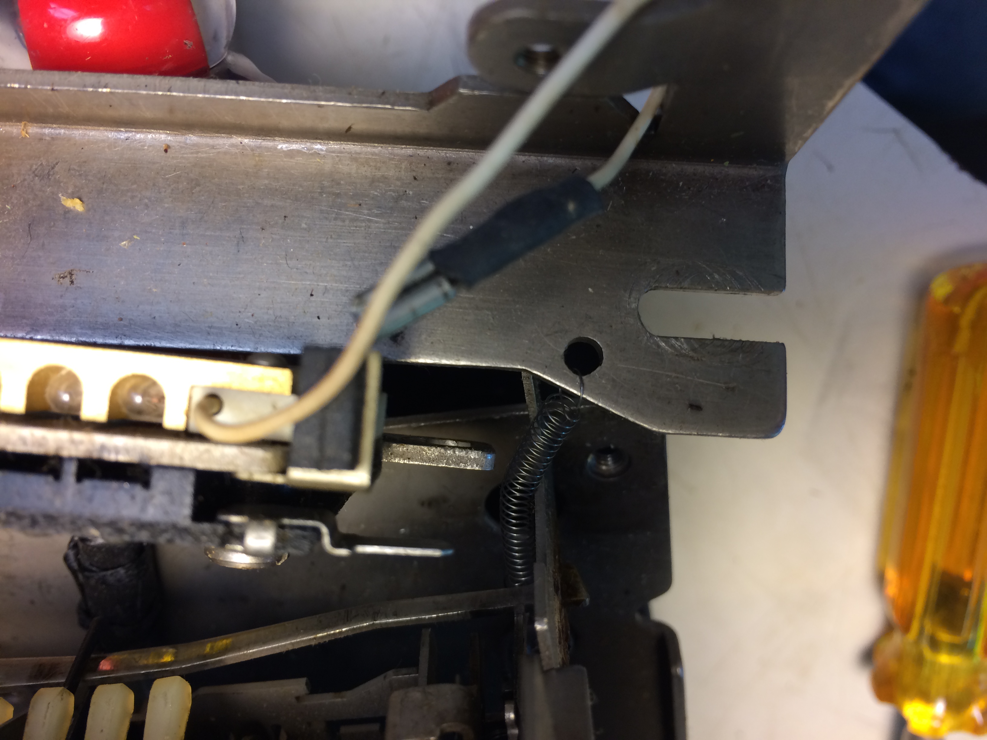
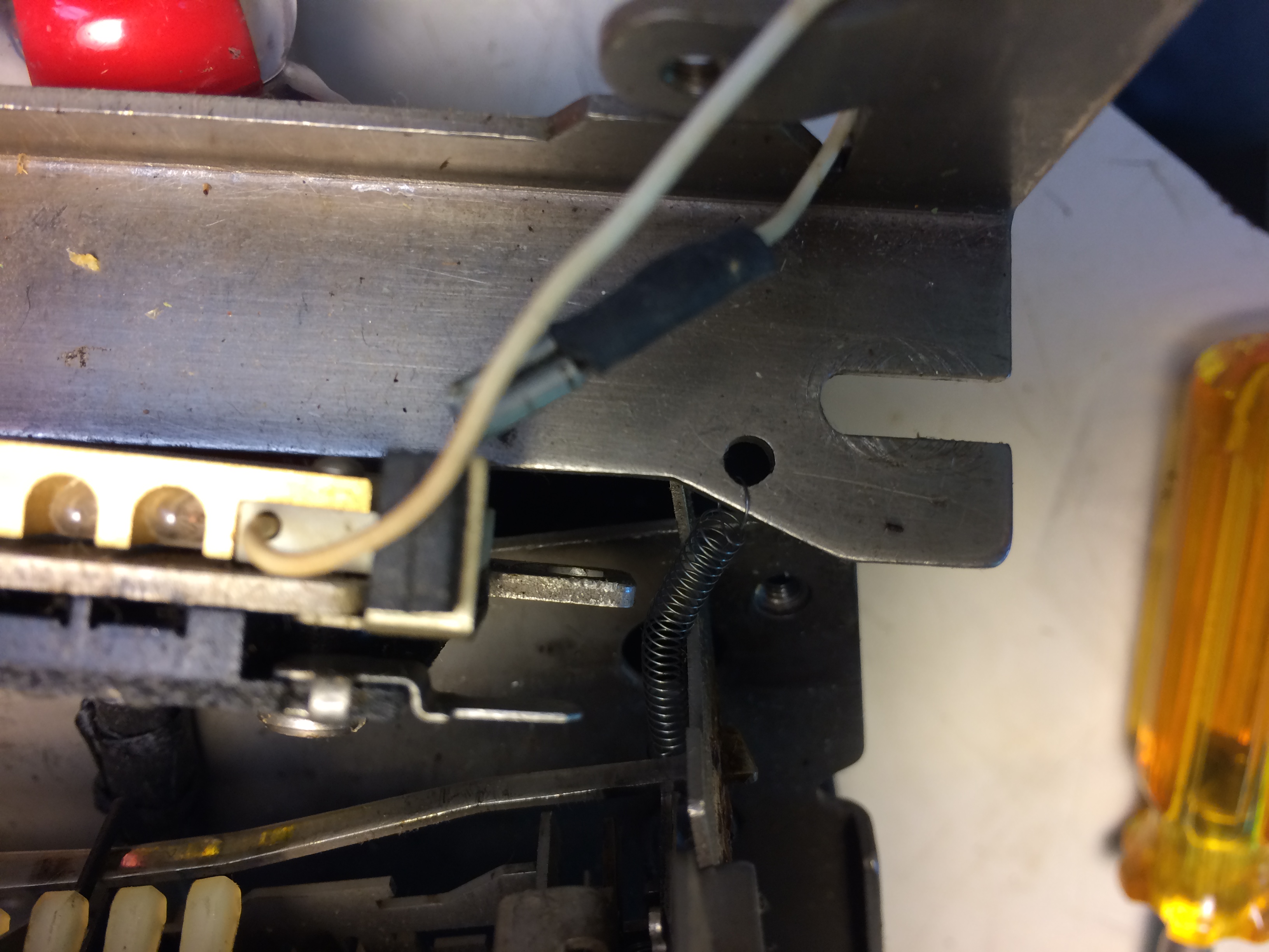
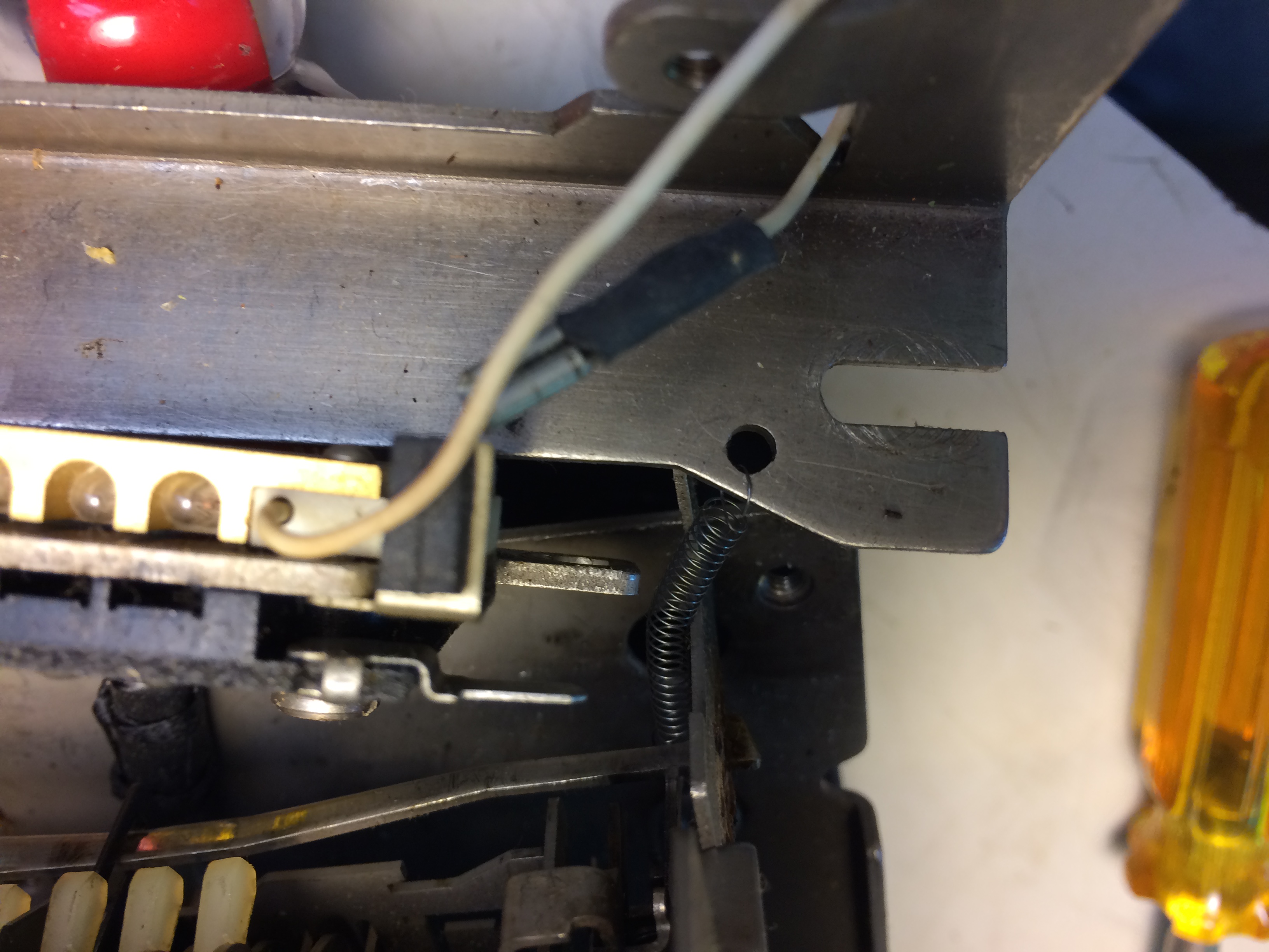
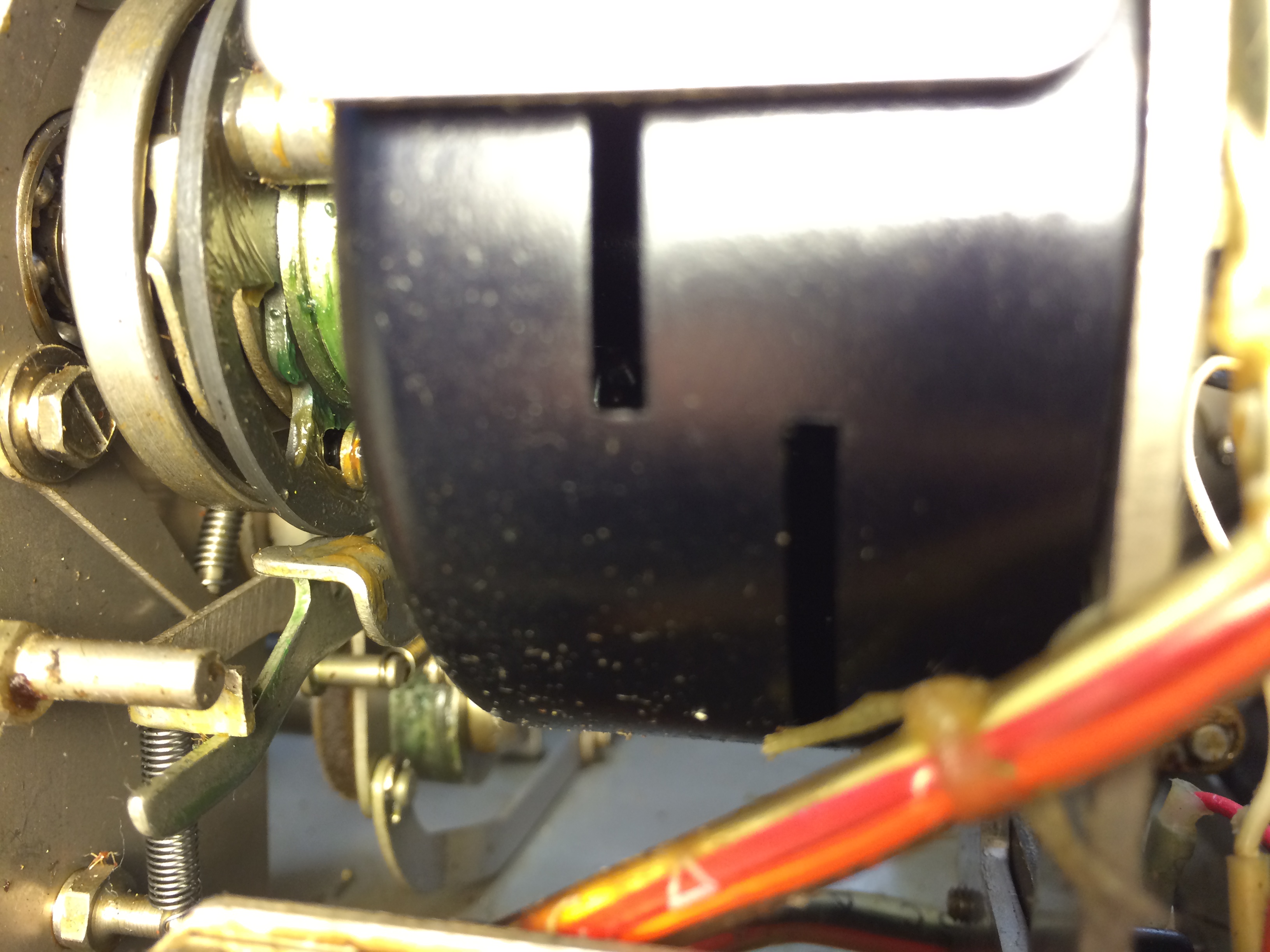
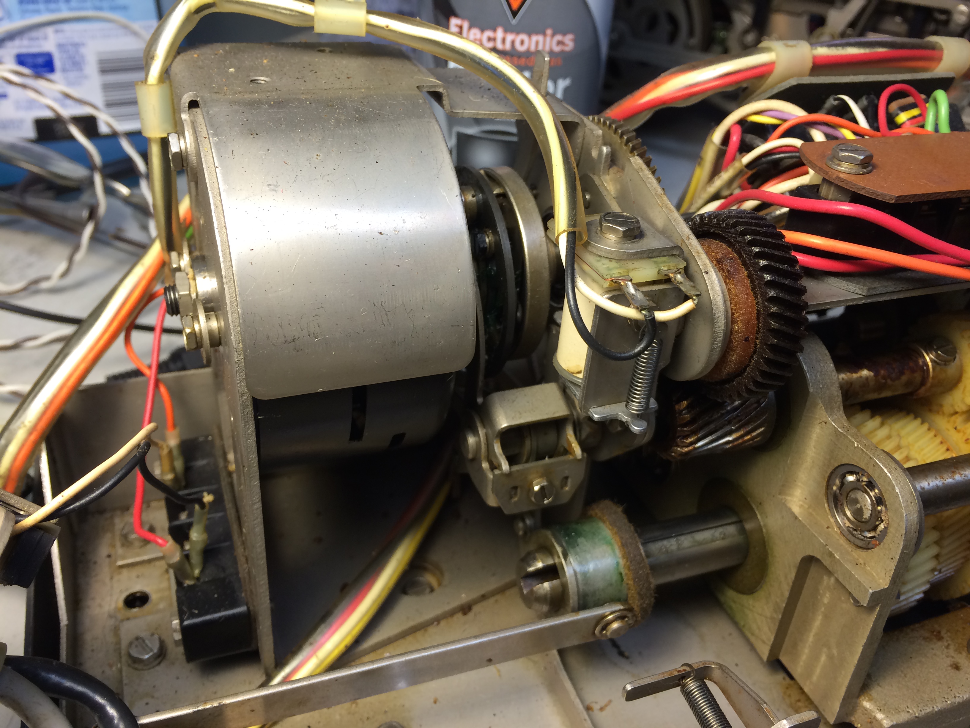
The RFI selector mechanism mounts on the upper right side frame of the typing unit. The selector consists of a special three-pin electrical receptacle, double shielded cable and metallic container.
The three-pin electrical receptacle insures a secure and shielded electrical connection to other associated apparatus,. The double shielded cable electrically connects the three-pin electrical receptacle to the selector magnets. The shielded cable is composed of three electrical conductors encircled by braided inner and outer shields. The inner and outer braided shields are electrically separated from each other and the three electrical conductors by flexible solid dielectric. The metallic container functions as a shielded enclosure for the selector magnet assembly.
Enclosed within the metallic container are the selector magnet coils, coil mounting bracket and selector armature. Each selector magnet coil contains an electrostatic shield which surrounds the coil windings. The selector coil mounting bracket provides mounting facilities for the coils, armature, and biasing spring. The receptacle, shielded cable, metallic container, and selector coils provide RFI suppression when used with associated RFI equipment.
SMD Schematic, SMD Card Assembly
The input current to the 323810 selector magnet driver (SMD) is a low level +6 volt for a marking state, and a -6 volt for a spacing state.
The output current of the SMD is 60 mA +/-10% during the marking state. The output is zero during the spacing state. Overall receiving margins of properly adjusted 28 type selectors driven by this SMD (polar rectangular wave input) should exceed 70 points at either input. The SMD operates at bit rates up to 75 baud.
The SMD assumes the marking state with positive input voltages not greater than 0.5 volt and the spacing state with negative voltages not greater than 0.5 volt. The marking and spacing switching levels are adjustable within 10% of each other. This requirement applies to either input. Each input of the SMD has a minimum input resistance of 50,000 ohms. The maximum input capacitance of either input is 2500 picofarads.
The SMD provides two inputs and makes possible reception from either one of two separate transmitters (single input operation) while the input line from the other transmitter is open. A spacing signal at either input will provide a spacing output. The SMD provides a marking output when both inputs are open. Both inputs cannot be in the marking condition simultaneously without producing a garbled output.
Circuit Description - The TP323810 selector magnet driver (SMD) is basically a direct coupled amplifier providing a current gain of approximately 80 db. The first two stages (Q1, Q6, or Q5, Q7) provide the necessary gain to drive a Schmitt trigger (Q8 and Q9). Q2, Q3, and Q4 comprise a power regulator stage which provides the power supply with a constant load .
In the marking state with a positive voltage with respect to common applied to each input (or a positive voltage on one input, the other open), Q1 and Q5 conduct, which in turn saturate Q6 and Q7. In this marking state the voltage drop from the emitter of Q6 to the collector of Q7 is less than the voltage drop from the CR15 anode to the Q8 emitter. Under this condition, the base-emitter junction of Q8 is reverse biased, thus turning Q8 off. With Q8 off, the Q9 base will conduct through R26 and thus energize the external selector magnet in the collector circuit. Transistor Q9 base current is sufficient to saturate the collector. In this condition, selector magnet current is determined primarily by the value of the limiting resistor R23 and the power regulator output voltage .
In the spacing state, with a negative voltage on input 1, input 2, or both inputs, the respective input transistor or transistors (Q1, Q5) are off. In this condition Q6-Q7 collector current is cut off and the base of Q8 conducts . Transistor Q8 base current is sufficient to saturate the collector. The Q8 emitter-collector saturation voltage is less than the forward drop across CR13 thus reverse biasing the base emitter junction of Q9. With this junction reverse biased, Q9 collector current is cut off and the selector magnet is de-energized.
Because of the difference in magnitude of Q8 and Q9 load currents, the drop across R21 will be greater in the marking state than in spacing. This means that the input voltage to the third stage (Q6 VCE + Q7 VCE) necessary to change the state of Q8 will be different depending on the previous state . Specifically, a larger combined Q6 and Q7 collector-emitter voltage is required to turn on Q 8 than to turn off Q8. This hysteresis, peculiar to Schmitt triggers, enables positive driver input signals to energize the selector coil and negative going input signals to de-energize the coil.
Resistors R4 , Rl6 , and potentiometers R3 and R15 serve to bias Q1 and Q5 and set the center of the switching interval . Emitter resistors R7 and R18 assist in gain stabilization. Resistors R6, R8 and R19, R20 form voltage dividers to bias CR2, 3, 4 and CR10, 11, 12. These diodes exhibit temperature characteristics such that together with R7 and R18, effective temperature compensation is obtained to stabilize the switching level of the SMD. Diode CR5 establishes a voltage reference for the first stages to insure switching level stability.
When low resistance transmitters (about 100 ohms) are used to key the driver, R1 and R13 have no significant effect on the operation of the circuit. However, when the line resistance is high (open line), R1 and R13 apply sufficient bias to drive Q1 and Q5 into conduction. This operation will maintain the terminal equipment in the idle state when input lines are open, or allow single line operation by simulating a marking signal on the other input.
In the power regulator, CR8 and the base-emitter junction of Q4 establish a voltage reference for R11 which determines the current drain of the unit . Diodes CR6, CR7, and the base emitter junction of Q3 serve to clamp the Q4 collector at a low voltage so as to minimize power dissipation in Q4. As the power requirement of the circuitry following the regulator decreases, the output voltage of the regulator will begin to rise. This rise corresponds to a decrease in Q4 collector-base voltage. The effect is to increase the forward bias on the base-emitter junction of Q3 and cause increased collector conduction. This collector current increases the conduct ion of Q2 whereby Q2 and R10 absorb the excess power. Q2 functions as a variable resistance so as to maintain a constant resistance across the output of the regulator regardless of the state of the driver circuitry. As a consequence of this, the power supply sees a constant load, regardless of driver state.
Capacitors C4 and C5 provide negative feedback to reduce transient generation in the driver. Capacitors C3 and C7 and C8 are radio frequency bypass capacitor s to eliminate any parasitic oscillations that may occur as a result of switching .
Circuit Description - Power supply transformer T1, diodes CR1, CR3, and power supply rectifier filter capacitor C8 form a full-wave rectifier to obtain a minimum of 58 volts unregulated dc.
Transistors Q1 and Q2 form a two-stage series voltage regulating element. Both transistors are always conducting, and the base emitter drop of each transistor is approximately 0. 7 volt. The voltage drop across R2 is negligible. (Resistor R2 is used in conjunction with capacitor C5 for RFI noise suppression.) In effect, then, the emitter of Q1 is clamped to the same potential as the reference diode combination CR7 and CR12 - i.e., the dc output of Q1 is nominally 47 volts. The difference between the Q1 dc output and the unregulated dc appears across the collector-emitter junction of Q l .
Transistor Q2 is a gain stage for Q l . Resistor R1 limits the current that divides between the CR7-CR 12 reference diodes and the base of Q2 . The base current of Q1 or the collector current of Q2 is equal to the base cur rent of Q2 multiplied by the de current gain (HFE) of Q2 .
Resistor R7 acts as a bleeder and assures that Q1 and Q2 will conduct even when no load is connected across the output terminals. Without R7 and no load connected, the output would rise to the same value as the unregulated dc . However , a minimum load of 0.150 ampere must also be applied to maintain the +53 volt regulation limit .
The +7 volt output is obtained by dropping the unregulated de voltage through resistor R4 to supply the zener reference diode C R6 which is connected across the output.
Resistor R5 and zener diode CR5 provide a - 7 volt output in a manner similar to that described above. However, a full-wave rectifier consisting of rectifier diodes CR2 and CR4 and capacitor C4 is required to obtain the negative unregulated potential with respect to the circuit common .
Capacitors C1, C2, and C3 suppress RFI noise transients which occur due to rectifier switching . Capacitors C6 and C7 and inductors L3 and L4 suppress zener diode noise .
The transformer shields and a low-pass filter consisting of L1, L2, C9, C10, C11 , and C12 provide noise isolation between power line and power supply .
The electrical service assembly is wired so that a 250 ohm (25 watt) resistor is connected across the collector-emitter of Q1 when the associated SMD is inserted in its connector to reduce power dissipation in Q1. (This is equivalent to paralleling Q1 with 250 ohms for each 0.150 ampere, approximately, of load current.)
Fuse F102 limits the output current to a total of 0.5 ampere.
 |
 |
 |
 |
 |
 |
 |
 |
 |
 |
 |
 |
 |
 |
 |
 |
 |
 |
 |
 |
 |
 |
 |
 |
 |
 |
 |
 |
 |
 |
 |
-- |
AN/UGC-20B |
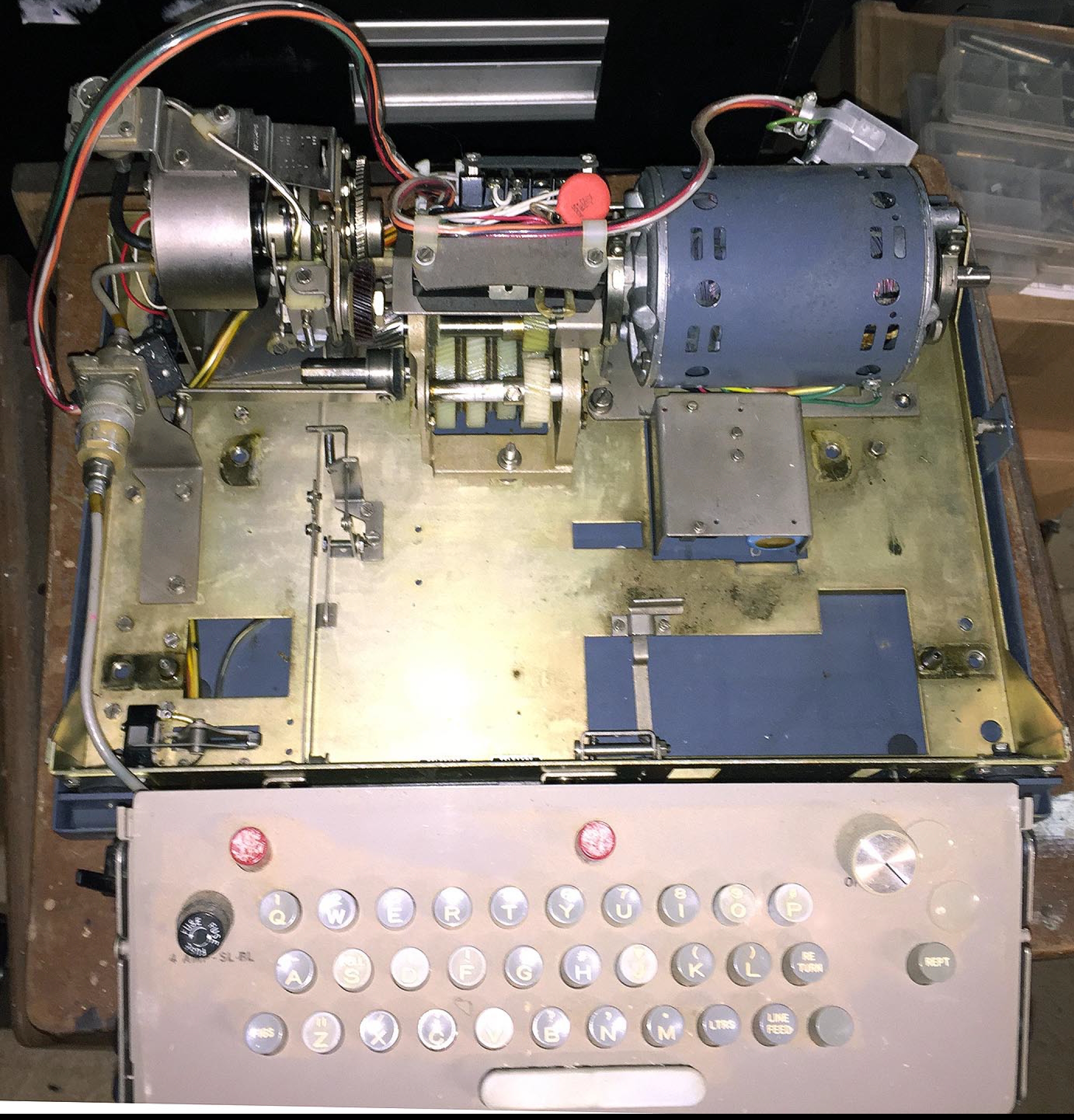
AN/UGC-20B is similar to AN/UGC-77 and has the same photoelectric keyboard
and distributor. Unlike the UGC-77, it has a built-in 60ma keyer (or can output 1.5v/70uA directly from the photocells). It does not have +/-6v output. |
|

